Lead Free PCB Assembly: A Sustainable and Reliable Manufacturing Standard
Lead free PCB assembly has become a global manufacturing standard as electronics manufacturers move toward environmentally responsible and regulation-compliant production. This assembly approach eliminates the use of lead-based solder and replaces it with safer alternatives that meet international environmental directives. As electronic devices become more advanced and widely used, lead free PCB assembly ensures both human safety and long-term product reliability without compromising electrical or mechanical performance.
Why Lead Free PCB Assembly Is Essential Today
Lead free PCB assembly is driven primarily by strict environmental and safety regulations such as RoHS and similar global compliance standards. These regulations restrict hazardous substances in electronic products to reduce environmental pollution and health risks. Manufacturers that adopt lead free processes not only meet regulatory requirements but also demonstrate a commitment to sustainability. Beyond compliance, lead free PCB assembly supports global market access, allowing products to be sold across regions without regulatory barriers.
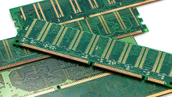
Materials Used in Lead Free PCB Assembly
The core difference in lead free PCB assembly lies in the solder material. Traditional tin-lead solder is replaced by lead free alloys, most commonly based on tin combined with silver and copper. These materials provide strong solder joints, excellent electrical conductivity, and long-term reliability. However, lead free solder has a higher melting point, which requires precise temperature control during the assembly process. This makes process optimization and equipment calibration critical to achieving consistent results.
Impact on PCB Substrates and Components
Lead free PCB assembly places higher thermal stress on both the PCB substrate and electronic components due to elevated reflow temperatures. As a result, materials such as high-Tg laminates and heat-resistant components are often selected to ensure durability. Proper material selection is essential to prevent issues such as warpage, delamination, or premature component failure.
Manufacturing Process of Lead Free PCB Assembly
The lead free PCB assembly process follows the same fundamental steps as conventional assembly, but with stricter control requirements. Solder paste printing must be highly accurate to ensure proper joint formation. Component placement precision becomes even more important due to the narrower process window of lead free soldering. Reflow soldering profiles are carefully developed to balance sufficient heat exposure with component safety.
Reflow Soldering Challenges and Solutions
One of the biggest challenges in lead free PCB assembly is managing the reflow soldering process. Higher peak temperatures increase the risk of thermal damage, making precise thermal profiling essential. Manufacturers rely on advanced reflow ovens and real-time monitoring to maintain consistent solder joint quality. Proper cooling rates are also critical to achieve optimal grain structure in the solder joints, which directly affects mechanical strength and reliability.
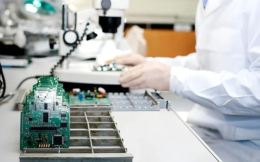
Quality Control in Lead Free PCB Assembly
Quality assurance is a key pillar of successful lead free PCB assembly. Inspection techniques such as automated optical inspection and X-ray inspection are widely used to detect solder defects that may not be visible to the naked eye. Functional testing ensures that assembled boards perform as intended under real operating conditions. Since lead free solder behaves differently from traditional solder, quality standards are adjusted to reflect acceptable joint appearance and performance characteristics.
Reliability Testing and Long-Term Performance
Products manufactured through lead free PCB assembly are often subjected to extensive reliability testing. Thermal cycling, humidity exposure, and mechanical stress tests help validate long-term performance. These tests are particularly important for applications in automotive, industrial, and medical sectors where failure is not an option. Properly executed lead free PCB assembly can achieve reliability levels equal to or even better than traditional leaded processes.
Industries Benefiting from Lead Free PCB Assembly
Lead free PCB assembly is now standard across consumer electronics, automotive systems, industrial equipment, medical devices, and telecommunications infrastructure. Consumer electronics brands rely on lead free processes to meet global compliance requirements. Automotive electronics benefit from improved solder joint strength under high-temperature conditions. Medical and industrial applications value the safety and reliability offered by lead free assembly, especially in mission-critical environments.
Cost Considerations in Lead Free PCB Assembly
While lead free PCB assembly can involve slightly higher material and process costs, these expenses are offset by regulatory compliance and global market access. As manufacturing technologies have matured, the cost gap between leaded and lead free assembly has narrowed significantly. Efficient process design, optimized sourcing, and experienced manufacturing partners help control costs while maintaining high quality.
Design Considerations for Lead Free PCB Assembly
Designing for lead free PCB assembly requires close collaboration between design engineers and manufacturing teams. Pad geometries, thermal reliefs, and component selection must be optimized to support reliable soldering. Proper design for manufacturability ensures higher yields, fewer defects, and smoother production scaling. Early consideration of lead free requirements helps avoid costly redesigns later in the product lifecycle.
Future Trends in Lead Free PCB Assembly
The future of lead free PCB assembly continues to evolve with advancements in materials, automation, and inspection technologies. Improved solder alloys, enhanced thermal management solutions, and smarter process monitoring systems are driving higher reliability and efficiency. As sustainability becomes a core focus across industries, lead free PCB assembly will remain a foundational manufacturing approach for modern electronics.
Conclusion
Lead free PCB assembly represents a responsible, compliant, and technically advanced solution for modern electronics manufacturing. It supports environmental sustainability, meets global regulatory standards, and delivers reliable performance across diverse applications. For companies seeking dependable production with full compliance and scalable capabilities, partnering with PCBA China provides access to advanced lead free PCB assembly expertise, efficient manufacturing infrastructure, and cost-effective solutions tailored for global markets.